LightSpeed
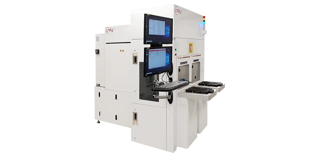
Defect Inspector solutionsThe LightSpeed is the world’s most flexible unpatterned defect inspection tool.
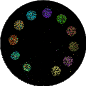
UnitySC’s elegant use of the principle of “Synchronous Doppler Detection“, allows inspection of both Opaque AND Transparent materials, with clear separation of Frontside vs Backside defects.
LightSpeed has the ability to find tiny defects at high speeds on both Compound/Glass Wafers AND the standard Silicon wafers that are often used for Process-Tool-Monitoring in fabs.
This 2-in-1 inspection ability allows customers to avoid buying 2x separate inspectors.
The LightSpeed can share an EFEM with other modules/tools, such as the PSD. This lowers costs, while allowing a “no compromises” implementation of 2x different Physics-techniques needed to detect your combination of issues.

Some Wafer types LightSpeed excels in
-
Opaque and Transparent wafers of all types:
-
SiC
-
Silicon
-
Glass/Fused-Silica
-
GaAs
-
GaN
-
Sapphire
-
InP
-
- Wafers of sizes from 2″ to 12″
- Wafers with a wide range of thicknesses, including Glass-on-Silicon 2wafer-bonded-stacks.
- Power Si Wafers, MEMS Si wafers, Glass Wafers (for Advanced Packaging, CIS & AR/VR), Compound wafers (all types), Wafer makers OQC, Chip makers IQC, etc.

