BIG NEWS!
Unity-SC is now part of the Electronics business of Merck KGaA, Darmstadt, Germany
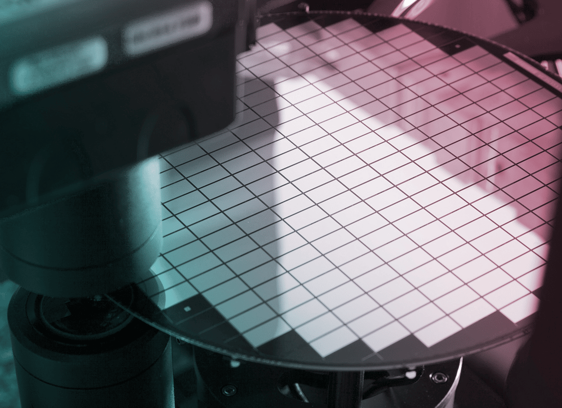
Where Metrology & Inspection Meet Materials Intelligence™
WE ENABLE OUR CUSTOMERS TO YIELD HIGHER & FASTER

WHO ARE UNITYSC?
UnitySC was formed in 2016, by a combination of European companies. Headquarted in France, UnitySC has a worldwide footprint, with staff in every major chip producing region.
WHAT DOES UNITYSC MAKE?
UnitySC is a leader in creating Metrology & Inspection tools used for Advanced Packaging (TSVs, High BandWidth Memory Chip stacks, Hybrid-Bonding/Wafer2Wafer, Die2Wafer) & MEM’s.
We also make equipment for unpatterend wafer defect inspection (all types of Compound-semi substrates like GaN, GaAs, InP, SiC, Glass, Sapphire, Ge, Silicon).
Plus other Metrology & Inspection equipment for other use-cases, all of which are used by our customers for yield improvement.

WORKING AT UNITYSC
At UnitySC, we promote and support from a diverse talent pool. We are pushing the frontiers of technology, making us an attractive place to work that allows all our employees to grow and succeed.

UNITYSC’S SERVICES
UnitySC are able to offer resources for Service & Applications Support for our equipment to customers all over the world.
We provide a comprehensive range of maintenance, upgrade and other services, depending on your requirements. Through these services, we can continuously maintain the health of your tools over their lifetimes.
Our Spare Parts Team offers a quick and reliable service to keep your production lines moving.
EXAMPLES OF OUR CUSTOMERS’ END MARKETS
Automotive
The move from ICE vehicles to E-vehicles, Autonomous driving (eg; ADAS), in-car-tech, digital connectivity & security. All these trends have one common enabler: Semiconductor components.

High-Bandwidth Memory (HBM)
High-Performance Computing (HPC)
AI-driven data analytics require real-time data processing at scale. UnitySC optimizes Semiconductor industry computing and memory architectures (GPU & CPU) for efficient handling of large and time-critical datasets.
Enhancing overall performance in data analytics, more efficiently and securely handled.

Internet Of Things
IoT technology in its ultimate form will consist of an ecosystem of securely hyperconnected devices driving the world of tomorrow. In short, more & more physical products will contain more & more chips of all types of functions.

AI & Augmented
Virtual Reality
Augmented reality and artificial intelligence are distinct technologies, but together they create unique digital experiences.
These technologies require smaller form factors, higher performance chip-materials and novel packaging approaches.

What’s new
Press releases
UnitySC Expands; Opens U.S. Office With Global Software Development Center And Customer Demo Lab
New Facility Enhances Company’s Semiconductor Process Control Capabilities and Supports Growing North America Customer Base Austin, Texas – Oct. 23, 2017 – UnitySC today announced at the International Wafer Level Packaging Conference (IWLPC) in San Jose, Calif., the...
UNITYSC RECEIVES MULTIPLE ORDERS FOR WAFER THINNING INSPECTION SYSTEMS
Leading IDM Selects New 4See Series Automated Defect Inspection Platform for Power Semiconductor Automotive Applications Grenoble, France, May 9, 2017 – UnitySC, a leader in advanced inspection and metrology solutions, today announced multiple orders from a leading...
Events
IWLPC
San Jose, CA Wafer Level Packaging is almost everywhere: smartphones, automotive, IoT, medtech, etc... Meet with us at IWLPC on booth #10 and listen to our talk entitled "Wafer Thinning In-Line Inspection Process Control Solution for High Volume Manufacturing". To...
IMAPS 2017
Raleigh, NC UnitySC will be exhibiting on booth #421 and delivering a talk entitled "In line Advanced Process Control Solution for the Fabrication of Micro-bumps". Come to meet with us. To pre-arrange a meeting, send us a message.
News
Unity SC (A FOGALE Nanotech Company) disclosed two new metrology solutions for advanced packaging applications
T-MAP 3D Time-domain Optical Coherence is the most robust solution for TSV depth, bow & warp and individual layer TTV of a stack measurement as each interface is detected in the right order over a larger range than spectral interferometry. The only limitation is...
Why Ultra Thin Power Semiconductors Calls For Advanced Inspection Process Control
Article published in Silicon Semiconductor (Volume 39, Issue 4 2017) Thin and ultrathin ICs are in high demand, but yield that sacrifices reliability has little value. Inspection process control can be the solution, according to UnitySC. By Gilles Fresquet, CEO,...